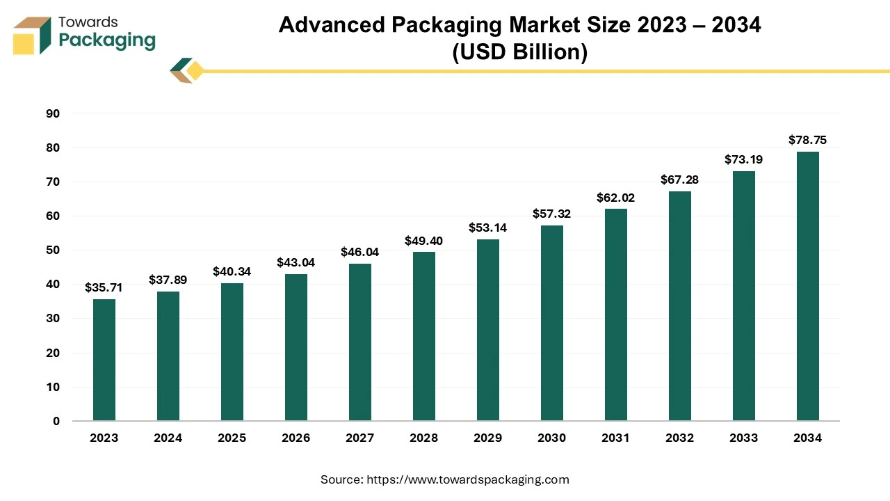
The global advanced packaging market is estimated to reach USD 78.75 billion by 2034, up from USD 35.71 billion in 2023, at a compound annual growth rate (CAGR) of 7.59% from 2024 to 2034.

Get All the Details in Our Solution – Download Brochure: https://www.towardspackaging.com/download-brochure/5390
The industry for advanced packaging is set to achieve substantial development in the years ahead. Multiple semiconductor chips are combined into a single chip package using a variety of manufacturing techniques known as advanced semiconductor packaging. This method lowers costs and power consumption while increasing capabilities. The most widely used methods in advanced packaging are system-in-package, fan-out wafer-level packaging, heterogeneous integration, 2.5D, and 3D-IC.
Placing chips with various functionalities close to one another has the added benefit of lowering power consumption, improving speed, and combining multi-function components into a single package. Large IDMs like Intel and Samsung, four sizable international OSATs, and the foundry and packaging company TSMC dominate the market for advanced packaging. Many advanced packaging platforms are being developed by these leaders. Every platform continues to gain a lot of popularity; however they all have unique qualities and possibilities.
The surge in demand for high-performance electronic devices such as smartphones, wearables, and IoT gadgets along with the growing adoption of technologies like 5G, artificial intelligence (AI) and the Internet of Things (IoT) are expected to augment the growth of the advanced packaging market during the forecast period. Furthermore, the miniaturization trends in the automotive sectors as well as shift towards the electric vehicles with autonomous driving systems are also anticipated to augment the growth of the market.
Additionally, the growing demand for the energy-efficient options in the data centers and cloud computing infrastructure coupled with the increasing investments in the semiconductor manufacturing and the growing government initiatives supporting domestic semiconductor production are also projected to contribute to the growth of the market in the near future.
Key Trends and Findings
- With the help of new technology, industry and academics are currently predicting a number of exciting megatrends. One of the newest innovations that has the potential to transform every industry area is artificial intelligence, which is driven by substantially improved algorithms and increasing processing performance. Autonomous driving is also one of the hottest subjects in the automobile industry right now. Sensing the car’s surroundings is one problem to address. As a result, a large number of MEMS sensors are required, which are enhanced by sophisticated packaging techniques. 5G communication is considered to be one of the key technology enablers for the aforementioned technology as well as the Internet of Everything.
- One of the main forces behind innovation in the electronics sector is the mobile market. Therefore, multi-camera systems, OLED display technology, 3D sensing, 5G modules, AI capability and AR/VR are important areas of electronics development. Every smartphone contains about 20 SiPs. For the application processor, three packaging types are frequently used Fan-Out PoP technology (exclusive to Apple), Flip Chip Package-on-Package, and Stacked-Die-in-Package. Deca Technologies is a supplier of iPhone components that specializes in a technology known as fan-out wafer-level packaging.
- The power of AI models to generate new information, material, or solutions on their own is demonstrated by the generative AI age. AP technologies provide the highly efficient hardware needed in the modern era, which can analyze massive volumes of data and produce complicated algorithms in real time.
- To support complicated communication networks, the introduction of 5G technology requires the utilization of small and effective devices. 5G devices benefit greatly from AP technologies like WLCSP and fan-out packaging, which makes possible smaller form factors, reduced power consumption, and better thermal management.
- A promising area for improved IC wafers and advanced packaging is represented by glass core substrates. For the next phase of chip designs and packages, they provide performance and scalability that are unmatched. As with all new technologies, there are still obstacles to overcome, but the combined efforts of both industry pioneers and upstarts are opening the door for glass substrates to be widely used in a variety of end industries, with AI chips and servers receiving special attention.
- North America held considerable market share of 29.87% in 2023. This is due to the advanced R&D capabilities and demand for cutting-edge technologies along with its focus on 5G infrastructure and AI applications.
- Asia-Pacific is expected to grow at a fastest CAGR of 9.66% during the forecast period owing to the strong semiconductor manufacturing base, government support and the presence of key players like TSMC, Samsung, and SK Hynix.
Invest in Our Premium Strategic Solution: https://www.towardspackaging.com/price/5390
Get the latest insights on packaging industry segmentation with our Annual Membership – https://www.towardspackaging.com/get-an-annual-membership
If you have any questions, please feel free to contact us at sales@towardspackaging.com
Browse our Brand-New Journal:
https://www.towardshealthcare.com
https://www.towardsautomotive.com
For Latest Update Follow Us: https://www.linkedin.com/company/towards-packaging/
Get Our Freshly Printed Chronicle: https://www.packagingwebwire.com/